


In ceramic substrate manufacturing, the inability to reliably distinguish between critical structural defects and benign cosmetic anomalies directly erodes profit margins. Modern electronics rely on flawless ceramic bases to dissipate heat and conduct power. Misclassifying a surface mark as a microcrack leads to unnecessary scrap. This generates expensive false rejects. Conversely, missing a true microcrack risks catastrophic field failures under extreme thermal or mechanical stress. High-reliability sectors cannot tolerate these false accepts.
This guide breaks down the structural differences between these anomalies. We evaluate current inspection methodologies used across the industry. You will also find a practical framework for selecting an inspection system. You will learn how to balance high-speed throughput with pinpoint accuracy. Ultimately, you can protect your yield while maintaining rigorous quality standards.
Defect Severity: Microcracks compromise structural integrity and propagate under stress; surface marks are typically shallow, cosmetic artifacts from handling or tooling.
The Contrast Challenge: The high reflectivity and complex grain structures of ceramics make traditional rule-based optical inspection prone to high false-reject rates.
Technology Shift: Effective ceramic substrate microcrack inspection increasingly relies on AI-driven machine vision to contextualize defect morphology, or ultrasonic testing for subsurface validation.
Evaluation Metric: The primary success criterion for an inspection upgrade is the reduction of the Overkill Rate (false positives) without increasing the Escape Rate (false negatives).
Quality assurance departments face a delicate balancing act. They must catch every fatal defect without discarding good products. Misclassifying ceramic defects heavily impacts your production efficiency. It artificially inflates your per-unit costs and degrades overall yield.
Rejecting functionally perfect substrates damages your profit margins. Harmless tooling marks often trigger automated optical alerts. Superficial scratches look severe under poor lighting. Discarding these acceptable units artificially lowers your yield. It forces your facility to produce more units to meet quota. This overproduction consumes extra raw materials. It also wastes valuable machine time and operator labor. Overkill rates directly undermine your manufacturing efficiency.
False negatives present a much graver danger. Microcracks act as severe stress concentrators. They pose massive risks in high-reliability applications. Aerospace components and EV power electronics demand flawless components. An undetected microcrack can cause substrate fracture. It may even trigger thermal runaway in battery systems. Such failures lead to massive product recalls. They introduce severe liability risks and permanently damage brand reputation. Escaping defects are unacceptable in zero-defect manufacturing environments.
A viable inspection solution must meet three critical benchmarks:
Speed: It must deliver repeatable classification at production line speeds. Units Per Hour (UPH) cannot drop.
Accuracy: It must consistently reduce overkill rates while keeping escape rates near zero.
Compliance: It must maintain strict compliance with industry-specific quality standards. These include IPC and MIL-STD regulations.
Meeting these criteria requires moving beyond subjective human inspection. You need automated, repeatable, and context-aware systems.
Understanding the physical nature of these anomalies is crucial. You cannot train an AI or configure an optical system without this knowledge. Microcracks and surface marks originate from entirely different processes. They also exhibit distinct morphological traits under magnification.
Microcracks threaten the physical stability of the entire substrate. They compromise dielectric strength and mechanical durability.
Root Causes: Thermal shock frequently causes these fractures. Uneven cooling during the sintering process generates massive internal stress. Mechanical stress during dicing or singulation also splinters the material. Aggressive laser cutting can induce micro-fractures along the cut edge.
Characteristics: These defects are typically deep and narrow. They often appear jagged or feature branching patterns. They penetrate deep into the substrate matrix. Because they disrupt the structural lattice, they have a high potential to propagate. Under thermal cycling, a small microcrack will expand until the substrate shatters.
Cosmetic anomalies look problematic but pose no functional threat. They do not penetrate the internal structure.
Root Causes: Handling abrasions are the most common culprit. Substrates rub against conveyor belts or automated grippers. Tooling friction leaves metallic residues on the ceramic face. Minor glaze or slurry inconsistencies also create visual discolorations.
Characteristics: Surface marks are usually shallow and wide. They exhibit uniform patterns rather than jagged edges. They remain confined strictly to the top surface layer. They have absolutely no impact on dielectric strength. They do not weaken the mechanical durability of the final component.
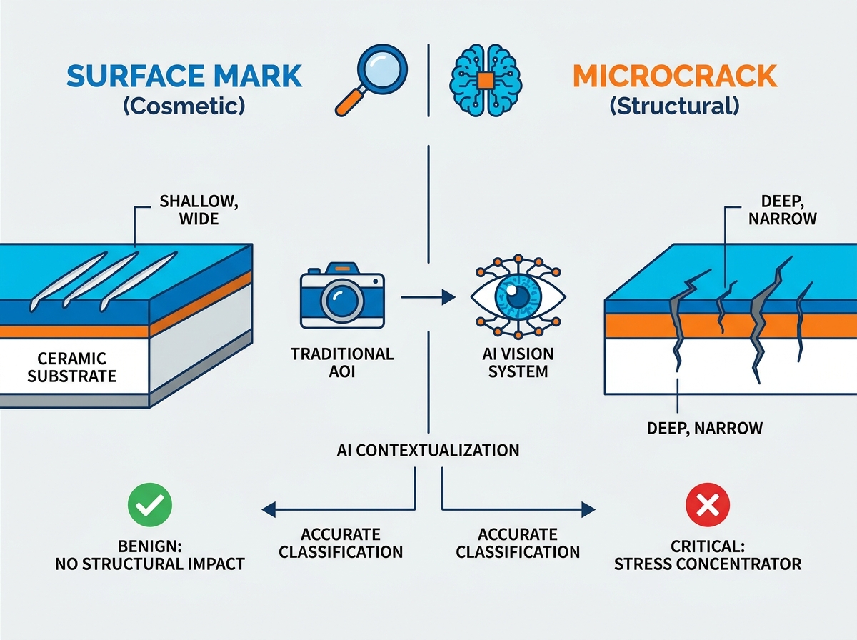
Implementing effective ceramic substrate microcrack inspection involves overcoming significant physical hurdles. Ceramics behave very differently from metals or plastics under inspection lighting. Their optical properties actively fight against standard vision cameras.
Alumina and aluminum nitride substrates are highly reflective. They feature complex, crystalline grain structures. These materials scatter incident light unpredictably. This unpredictable scattering causes harsh shadows across the surface. These shadows easily mimic the dark lines of real cracks. Conversely, excessive glare washes out shallow defects entirely. Standard ring lights usually fail on these materials. You need advanced illumination to penetrate the glare.
Hairline microcracks lack visual distinction. They often share the exact same grayscale values as surrounding ceramic grain boundaries. Traditional Automated Optical Inspection (AOI) relies on pixel-contrast rules. If a pixel is darker than a threshold, the system flags a defect. Because grain boundaries and microcracks share similar darkness levels, rule-based algorithms fail. They defeat standard edge-detection tools, causing massive false reject spikes.
Early-stage microcracks are incredibly small. They may be only a few microns wide. Detecting these anomalies requires extremely high-resolution optics. However, high-resolution cameras inherently reduce the Field of View (FOV). A smaller FOV means the camera must take more pictures to cover one substrate. This drastically slows down inspection times. Balancing micron-level detection with high-speed production remains a primary engineering challenge.
Choosing the right inspection technology determines your success. Different systems target different types of anomalies. You must align your technology choice with your specific quality requirements.
Comparison of Ceramic Inspection Technologies
Technology | Primary Strengths | Key Limitations | Best Use Case |
|---|---|---|---|
Traditional AOI | High speed, easy rule setup, cost-effective. | High false rejects on low-contrast defects. | Detecting gross defects or missing metallization. |
AI / Deep Learning | Contextual understanding, distinguishes marks from cracks. | Requires robust datasets and training time. | High-accuracy inline surface inspection. |
Ultrasonic (SAM) | Detects hidden internal voids and deep subsurface cracks. | Slow throughput, often requires water coupling. | Offline batch sampling or failure analysis. |
Traditional AOI excels at high-speed baseline checks. It is best for detecting gross defects. You should use it to find missing metallization layers or large edge chips. However, it has severe limitations. AOI relies entirely on rigid pixel-contrast rules. It frequently confuses harmless surface marks with fatal microcracks. This confusion forces manufacturers to implement manual secondary reviews. Human operators must double-check every rejected part, which slows down the entire facility.
AI systems represent a massive leap forward. They are best for high-accuracy ceramic surface mark detection. They easily distinguish complex crack morphologies from benign scratches. Deep learning models use neural networks trained on classified image datasets. They understand visual context much like a human inspector. They recognize the branching pattern of a crack versus the straight drag of a tool mark. They perform this analysis at machine speed. The main limitation is data preparation. You require a robust, well-labeled dataset. You must feed the model examples of both true defects and acceptable variations to train it effectively.
Ultrasonic Non-Destructive Testing (NDT) looks beneath the surface. It is best for detecting internal voids. SAM finds delamination and subsurface microcracks completely invisible to optical cameras. It sends high-frequency sound waves into the ceramic matrix and measures the echoes. While highly accurate, it has major limitations. SAM is typically much slower than optical methods. It often requires immersing the substrate in water.
Buying an advanced inspection system is only the first step. You must integrate it seamlessly into your existing workflow. Evaluating vendors requires looking past marketing claims. You must focus on practical deployment realities.
Space on a manufacturing line is always at a premium. Assess whether the new solution can be retrofitted onto existing handling equipment. Can the camera arrays mount above your current conveyors? If not, you will require a standalone inspection cell. Standalone cells take up more floor space. They also require additional robotic handlers to load and unload the substrates. Factor these footprint and handling requirements into your upgrade timeline.
AI solutions require ongoing management. Evaluate the vendor's software usability closely. Can your existing QA team train and update the models? You should not need to hire a dedicated data scientist. The best systems offer intuitive, no-code interfaces. They allow quality engineers to highlight defects on a screen and retrain the model instantly. Look for vendors who utilize transfer learning. This technique requires far fewer images to baseline a new product line.
Software cannot fix bad image capture. If the defect is invisible in the raw photo, AI cannot find it. Acknowledge this reality early. Ensure the vendor specifies specialized illumination tailored to ceramic surfaces. Ask about multi-angle structured light. Request darkfield illumination to highlight crack edges. Request coaxial lighting to flatten reflective glare. The hardware must create optical separation before the software analyzes the image.
Never buy an inspection system off a standard spec sheet. Demand a rigorous Proof of Concept (PoC). Send the vendor your own production samples. Specifically, send them the edge-case parts. Include the exact substrates that historically confuse your human inspectors. If the automated system can correctly classify your hardest parts, it will handle normal production easily. A physical PoC is the only way to validate true capability.
Distinguishing between a terminal microcrack and a benign surface mark is no longer a persistent bottleneck. You do not need to rely on slow, subjective human inspection.
Upgrading to advanced, context-aware inspection systems transforms your QA department. It shifts QA from a traditional cost center into an active yield-protection mechanism.
AI-driven machine vision successfully navigates the complex optical properties of ceramics, drastically lowering overkill rates.
Audit your current false-reject rates immediately. Quantify how much good product you throw away daily.
Consult with specialized inspection vendors to arrange a sample evaluation. Use this baseline data to calculate your potential ROI accurately.
A: High-resolution optics combined with AI can detect cracks down to 5-20 microns. Achieving this requires precise control over the field of view. It also demands specialized lighting setups, such as darkfield illumination, to create necessary contrast along the crack edges.
A: No. Machine vision is strictly for surface and near-surface defects. It relies entirely on reflected light. Ultrasonic testing (SAM) remains absolutely required to detect deep internal voids or subsurface structural anomalies hidden beneath the opaque ceramic layer.
A: Vendors often use techniques like transfer learning or synthetic data generation to overcome image scarcity. Additionally, many modern systems deploy anomaly detection models based on unsupervised learning. These models only require images of "good" substrates to successfully flag any unexpected deviations.
A: Yes. High surface roughness creates significant optical noise under standard lighting. Overcoming this requires multi-directional lighting to cancel out shadows. You also need deep learning algorithms specifically trained to ignore the substrate's natural texture while highlighting true anomalies.


