


Ceramic substrates like Aluminum Nitride (AlN) and Alumina (Al2O3) play a critical role in high-power, high-frequency, and extreme-temperature applications. You will find them driving EV power modules and cutting-edge RF communications where thermal management remains strictly non-negotiable. However, a major quality control problem plagues the industry. Standard FR-4 optical inspection protocols fail miserably on these advanced ceramics. High surface reflectivity, low metallization contrast, and unique material brittleness easily blind conventional inspection machines. Using standard equipment inevitably leads to dangerous missed defects or an overwhelming number of false alarms.
This guide establishes a standardized, evidence-based framework for evaluating AOI equipment and vendor capabilities. We will help you thoroughly validate machine capabilities before you commit to large capital expenditures or long-term outsourcing agreements. You will learn exactly how to structure rigorous test batches, define clear defect taxonomies, and analyze final acceptance reports.
Ceramic substrates require specialized multi-angle or coaxial lighting due to aggressive surface glare and low metallization contrast.
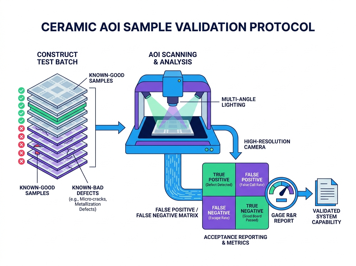
A rigorous AOI sample validation process must include a balanced mix of "known-good" boards and a comprehensive "known-bad" defect library.
Acceptance reports must clearly quantify the trade-off between Escape Rate (false negatives) and False Call Rate (false positives) using industry-standard Gage R&R metrics.
Deploying specialized acceptance testing protocols goes far beyond basic compliance. We must address the catastrophic nature of field failures. Micro-defects in Direct Bonded Copper (DBC) or Direct Plated Copper (DPC) ceramics actively compromise thermal conductivity. If an EV inverter power module contains a micro-void in its substrate metallization, heat cannot escape efficiently. The module eventually destroys itself under peak loads. Preventing these costly field escapes requires specialized equipment tailored to the distinct physical properties of ceramics.
Optical realities dictate a completely different inspection approach compared to traditional organic boards. Standard FR-4 printed circuit boards usually feature matte solder masks. They provide high contrast against copper traces. Ceramic substrates lack this convenient contrast. Bare alumina and aluminum nitride surfaces create intense glare and specular reflection under standard LED ring lights. Standard cameras misinterpret this intense glare as bridging shorts or extraneous copper.
Applying standard PCB inspection rules to highly reflective ceramics immediately triggers extreme false call fatigue. Standard rule-based algorithms flag hundreds of imaginary defects per panel. Operators must then manually review every single flagged location. Reviewing endless false positives rapidly exhausts human operators. They become desensitized and inevitably approve true functional defects simply to clear the backlog. Establishing specialized acceptance criteria stops this dangerous cycle by proving the machine can differentiate between harmless glare and actual flaws.
Selecting the right testing samples guarantees the integrity of your evaluation. A reliable AOI sample validation requires carefully curated panels representing normal production variance, not just "golden boards." Perfect panels tell you nothing about a machine's true production readiness. You must gather substrates exhibiting normal batch-to-batch color shifts, minor grain variations, and allowable metallization thickness differences.
To accurately stress-test detection limits, you must construct a comprehensive "known-bad" defect library. Do not rely entirely on theoretical software simulations. You need physical edge-case defects. Source or purposefully manufacture panels containing hairline fractures, subtle copper oxidation, and microscopic edge chips. We recommend following a strict sequence when running the evaluation:
Assemble fifty standard production panels showing normal process drift.
Integrate twenty purposefully flawed panels from your known-bad library.
Map the exact coordinates of every known defect before inserting them into the machine.
Run the complete mixed batch through the machine blindly.
Finally, always establish an un-optimized baseline. Force the vendor to scan your mixed sample batch multiple times using their default, out-of-the-box ceramic algorithms. Record this baseline data before allowing their engineers to tweak lighting settings or adjust sensitivity thresholds. Comparing the un-optimized baseline against the final tuned results reveals how much custom engineering your specific product will require moving forward.
Clear pass/fail criteria prevent costly arguments during final machine sign-off. Documenting exact tolerances for the ceramic substrate AOI acceptance test aligns vendor promises directly with your production realities. You cannot accept vague promises regarding defect detection. Every single anomaly must fall into a strictly defined category.
Substrate-level defects require highly specific metrics. Ceramics are notoriously brittle. Laser profiling and singulation processes often cause microscopic edge chipping. You must define exactly how many microns of chipping remain acceptable before a panel fails. Furthermore, the system must detect structural micro-cracking without falsely flagging natural ceramic grain boundaries as scratches. Surface contamination must trigger alarms, but harmless water spots might remain acceptable.
Metallization and circuit defects also demand rigorous thresholds. High-density interconnects on ceramics often utilize fine line/space widths. The machine must accurately measure copper peeling, trace over-etching, and bridging shorts. High-frequency RF applications cannot tolerate even minor trace neck-downs, as they alter impedance. You must clearly define these physical tolerances for the vision system.
Handling ambiguity remains the hardest part of taxonomy definition. You must separate harmless cosmetic anomalies from true functional defects. Slight copper discoloration might look ugly but perform perfectly. Severe oxidation, however, prevents proper wire bonding downstream. Your taxonomy must clearly dictate how the algorithm handles these ambiguous visual differences.
Defect Category | Specific Anomaly | Pass/Fail Threshold Example |
|---|---|---|
Substrate Integrity | Edge Chipping | Fail if chip depth exceeds 50 microns from the cutting edge. |
Substrate Integrity | Micro-cracking | Fail any continuous crack exceeding 0.1mm in length. |
Metallization | Trace Neck-down | Fail if trace width reduces by more than 15% of nominal design. |
Metallization | Copper Peeling | Fail any visible separation between the copper layer and ceramic base. |
Surface Contamination | Oxidation | Fail dark oxidation in wire-bonding zones; pass light discoloration elsewhere. |
Hardware specifications directly dictate inspection performance on advanced materials. Illumination architecture serves as the most critical hardware component. Standard top-down LED rings fail on glossy alumina. Defeating intense specular reflection requires highly specialized hardware configurations. When evaluating a machine, look for these specific illumination capabilities:
Coaxial Lighting: Projects light perfectly perpendicular to the substrate, eliminating shadows and highlighting flat reflective surfaces.
Multi-Spectral LEDs: Utilizes different wavelengths (red, green, blue, UV) to highlight distinct material layers, such as exposed ceramic VS plated gold.
Programmable Multi-Angle Domes: Casts diffuse light from various low angles to identify raised defects, peeling copper, and subtle surface scratches.
Camera and resolution requirements must match your specific design rules. Standard 15-micron pixel resolution cannot adequately inspect fine-pitch RF ceramic circuits. If your manufacturing process utilizes line/space widths below 20 microns, you need sub-micron optical resolution capabilities. High-resolution line-scan cameras combined with telecentric lenses prevent image distortion at the panel edges, ensuring consistent measurement accuracy.
You must carefully assess AI and deep learning integration claims. Many vendors use AI as a marketing buzzword. However, authentic deep learning profoundly transforms ceramic inspection. Rigid, rule-based algorithms struggle to interpret natural ceramic grain variations. Modern deep learning models excel at classifying these ambiguous visual patterns. They effectively suppress false calls by learning the subtle differences between a harmless natural grain line and a catastrophic micro-crack.
Implementation risks accompany these advanced AI capabilities. Deep learning introduces a steep learning curve. Training neural networks requires substantial data overhead. If you run a low-volume, high-mix production line, you might not generate enough defective samples to train the AI properly. Furthermore, heavy AI processing can significantly increase image analysis time. You must ensure the onboard computing hardware can handle the algorithmic load without causing bottlenecks.
The final acceptance report serves as your ultimate proof of machine reliability. Do not accept simple "pass/fail" summary emails. You need a comprehensive Gage R&R (Repeatability and Reproducibility) study. Gage R&R provides the mathematical proof of system stability. Repeatability confirms the machine gives the exact same result when it scans the same ceramic panel ten times in a row. Reproducibility confirms the results remain consistent even when different operators load the panels across different shifts.
You must transparently document the False Positive vs. False Negative Matrix. Every inspection system makes compromises. If you tighten the thresholds to catch every tiny micro-crack (reducing false negatives), you will inevitably flag more harmless dust particles (increasing false positives). The report must plot this exact percentage tradeoff. Note: A vendor claiming 0% escapes and 0% false calls on complex ceramics is statistically improbable. Demand to see the raw data backing up their claims.
Cycle time verification remains highly critical. A machine that catches 100% of defects but takes five minutes to scan a single panel holds no value in mass production. Ensure the equipment meets your required units-per-hour (UPH) targets without sacrificing its baseline detection accuracy. During testing, run the machine at its maximum rated speed and verify the escape rate does not artificially spike due to camera blurring or processing lag.
Finally, verify robust data traceability. Modern intelligent manufacturing demands seamless data flow. Verify the system can export high-resolution defect images instantly. It must coordinate bounding-box data and coordinate maps seamlessly into your existing MES (Manufacturing Execution System) or ERP platforms. Reliable integration enables downstream Statistical Process Control (SPC) engines to identify negative yield trends before they escalate into massive scrap events.
Your final shortlisting logic should rely entirely on empirical evidence. Never purchase or contract ceramic inspection equipment based on glossy spec sheets alone. Ceramics present unique optical challenges that standard PCB algorithms simply cannot overcome. By utilizing structured test batches, strict defect taxonomies, and rigorous Gage R&R metrics, you protect your production line from catastrophic field escapes and operator fatigue.
Your immediate next step is demanding a live, documented demonstration. Force the vendor to use your specific ceramic substrate samples, including both good boards and edge-case defects. Do not allow them to test using their own pre-optimized demo panels. Require them to provide a comprehensive statistical report proving their system can meet your required UPH targets while maintaining an acceptable false call rate.
A: No. X-ray (AXI) is required for discovering hidden voids in solder joints or via fills. However, optical inspection remains strictly mandatory for high-speed surface defect detection, scratch identification, and trace measurement. The two technologies are complementary, not interchangeable.
A: While highly dependent on product complexity, a well-tuned system utilizing deep learning on ceramics typically aims for less than 3-5% false calls. Initial setups may start much higher until the algorithms learn your specific production variance.
A: Depending on the complexity of your defect taxonomy and AI training requirements, a proper validation phase typically spans 2 to 4 weeks. This allows enough time for iterative testing, physical sample runs, and necessary algorithmic tuning.


