


Power electronics and RF module manufacturing operate in a high-stakes environment. Here, even minor substrate failures rapidly lead to catastrophic thermal or electrical breakdowns. For years, manufacturers relied heavily on manual microscopic inspection to catch these critical flaws. However, human operators inevitably suffer from eye fatigue, inconsistent judgment, and unacceptably low throughput. You simply cannot scale high-volume precision using manual methods alone. This operational bottleneck makes transitioning to Automated Optical Inspection mandatory for modern fabrication lines. This guide breaks down how you should configure and evaluate AOI systems effectively. We explore how to handle the distinct optical properties of Alumina, Aluminum Nitride, and Silicon Nitride substrates. You will learn proven strategies to optimize your inspection logic. Ultimately, you can improve detection accuracy without inflating costly false-reject rates.
Effective ceramic substrate AOI inspection requires material-specific optical configurations; a one-size-fits-all lighting setup will result in high false positive rates.
Al2O3, AlN, and Si3N4 each present unique imaging challenges, ranging from translucency and glare (Al2O3) to low contrast and dark backgrounds (AlN, Si3N4).
Reliable ceramic substrate defect detection must account for both bare substrate flaws (micro-cracks, pinholes) and metallization/bonding defects (DBC/AMB voids, etching errors).
Evaluating an AOI solution should prioritize false-call mitigation algorithms, automated handling safety, and integration capabilities with existing manufacturing execution systems (MES).
Power module fabrication demands absolute precision at every step. Implementing automated ceramic substrate defect detection fundamentally protects your manufacturing margins. The primary financial baseline relies on balancing yield protection against false rejects. AOI systems aim to find defects efficiently. However, you must also minimize "over-killing." Over-killing means rejecting perfectly good substrates due to strict system sensitivities. Over-rejecting directly erodes margins on highly expensive materials like Aluminum Nitride and Silicon Nitride. An optimized optical inspection system distinguishes true anomalies from acceptable cosmetic variations seamlessly.
Catching defects early ensures vital downstream reliability for your products. A tiny edge chip at the substrate level might seem trivial initially. Yet, it often causes expensive field failures in final power modules like IGBTs or SiC MOSFETs. We must intercept these issues before encapsulation or wire bonding begins. Identifying a flaw early prevents manufacturers from adding expensive silicon components to a doomed substrate.
Furthermore, strict industry regulations require comprehensive compliance and traceability. Automotive frameworks, such as IATF 16949, mandate rigorous quality documentation. Aerospace standards demand equally stringent production records. AOI systems meet these requirements through automated image archiving and precise defect mapping. They build a reliable digital twin of your production quality. This archived data allows you to prove compliance during supplier audits easily.
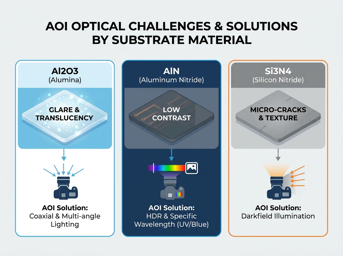
Different ceramics interact physically and optically in unique ways. You cannot use a universal lighting setup for all substrate materials. Reliable ceramic substrate AOI inspection must adapt to specific optical physics continuously.
Alumina heavily scatters incoming light. Its crystalline structure creates a semi-translucent surface layer. This translucency causes traditional direct lighting to bounce unpredictably. Consequently, the camera sensor often captures excessive glare or blurred trace edges. To correct this issue, your AOI requires specific hardware adjustments immediately. You should use coaxial lighting combined closely alongside multi-angle illumination. Coaxial light penetrates the ceramic surface slightly without blowing out the image sensor. Multi-angle LEDs help define surface topology clearly. This prevents false positives caused by subsurface grain reflections.
Aluminum Nitride presents a completely different inspection hurdle. AlN typically exhibits a darker, opaque appearance naturally. This dark background severely reduces the visual contrast between the bare ceramic and etched copper traces. Traditional cameras struggle to find distinct boundary lines accurately. To overcome low contrast, you must configure specific AOI hardware adjustments. High-dynamic-range (HDR) imaging becomes absolutely essential here. HDR merges multiple varying exposures to reveal hidden trace details. Additionally, using specific wavelength lighting improves visibility drastically. Deploying blue or UV light enhances surface edge detection significantly. These shorter wavelengths scatter less, providing crisp outlines on opaque backgrounds.
Silicon Nitride boasts exceptionally high fracture toughness. Despite this impressive mechanical strength, it remains susceptible to hard-to-see micro-cracks. Si3N4 also features notable surface texture variations. The matte grey or dark background hides topographical anomalies extremely well. Detecting fine scratches against this rougher texture challenges standard optics daily. Your AOI adjustments must include robust darkfield illumination. Darkfield lighting angles the light source very close to horizontal. This technique highlights topographical anomalies perfectly. Any scratch or micro-crack catches the low-angle light and shines brightly against the dark background.
Optical Characteristics Summary Chart
Material Type | Primary Optical Challenge | Recommended Lighting Setup | Key Imaging Technology |
|---|---|---|---|
Alumina (Al2O3) | High translucency causing severe glare | Multi-angle and coaxial illumination | Anti-reflection optical filtering |
Aluminum Nitride (AlN) | Opaque surface causing low trace contrast | Short-wavelength (Blue/UV) LEDs | High-dynamic-range (HDR) imaging |
Silicon Nitride (Si3N4) | Rough texture hiding fine micro-cracks | Low-angle darkfield illumination | High-resolution topographical scanning |
Proper imaging only solves half the inspection problem. You must also establish robust detection logic to interpret those captured images accurately. We divide the primary targets into bare ceramic anomalies and metallization flaws.
Inspecting the unbonded substrate requires hunting for inherent structural weaknesses proactively.
Cracks and Edge Chipping: Mechanical damage often occurs during singulation or dicing processes. Your inspection logic requires edge-specific lighting to catch these tiny fractures. Cameras positioned at oblique angles monitor the perimeter for jagged chips continuously.
Pinholes : Finding structural compromises demands extreme precision. This task requires transmitted light to shine completely through the material. Alternatively, you can deploy high-resolution top-down imaging. The software flags any dark spots indicating missing ceramic material automatically.
Contamination and Stains: Manufacturing environments inevitably introduce foreign particles. The detection algorithm must differentiate between harmless discoloration and critical foreign material. Color-based thresholding helps filter out acceptable processing stains from actual destructive debris.
Once copper bonds directly to the ceramic, new defect classes emerge. Direct Bonded Copper (DBC) and Active Metal Brazing (AMB) processes introduce distinct anomalies.
Copper Peeling and Delamination: Extreme heat stress causes copper layers to detach slowly. Identifying these blister-like formations requires advanced volumetric techniques. 3D AOI or structured light projects grid patterns onto the target surface. Distortions in the grid reveal unacceptable height variations caused by internal delamination.
Etching Flaws (Shorts/Opens): Chemical etching processes often leave unwanted copper or remove too much material. We deploy standard 2D geometric rule-based algorithms here. The software measures trace widths and spacing accurately. It verifies all dimensions stay safely within design tolerances.
Oxidation: Excessive surface oxidation degrades soldering performance later. We use color-based inspection logic to detect unacceptable levels of copper oxidation. The system rejects panels showing dark brown or purple hues exceeding established thresholds.
Standard Defects Evaluation Table
Defect Category | Specific Flaw | Required Inspection Logic |
|---|---|---|
Bare Ceramic | Edge Chipping | Oblique angle camera monitoring |
Bare Ceramic | Pinholes | Transmitted light or top-down scanning |
Metallization | Delamination | 3D structured light projection |
Metallization | Etching Shorts | 2D geometric rule algorithms |
Procuring an inspection system requires careful technical vetting. You must assess how well the hardware and software handle brittle, high-value components.
Programmable, multi-zone, multi-color LED lighting represents a non-negotiable hardware requirement. Mixed-material production lines frequently switch between Alumina and Silicon Nitride batches. You cannot afford to physically change light domes for every single batch. Software-controlled illumination allows instant recipe changeovers. This flexibility maintains high throughput while optimizing optical contrast for each specific substrate type.
Engineers constantly balance imaging detail against manufacturing speed. You need sub-micron resolution to catch dangerous hairline cracks reliably. However, high-resolution scanning slows down cycle times considerably. You must meet the strict Units Per Hour (UPH) requirements of high-volume manufacturing. We recommend calculating the smallest critical defect size first. Then, select a camera sensor mapping exactly three to four pixels to that defect. This ratio ensures reliable detection without processing unnecessary image data.
Modern platforms combine two distinct analytical approaches to maximize accuracy.
Rule-based logic: This traditional approach remains best for strict geometric measurements. It excels at verifying trace widths, checking keep-out zones, and ensuring pad alignments. The logic follows rigid mathematical parameters perfectly every time.
AI and Deep Learning: Artificial intelligence becomes crucial for classifying subjective defects accurately. It learns the subtle differences between scratch severity levels. AI easily distinguishes a harmless water stain from a critical electrical burn mark. Utilizing deep learning actively drives down false positive rates.
We must thoroughly assess the physical integration capabilities. Ceramics are notoriously brittle materials. The AOI machine must feature low-stress clamping mechanisms exclusively. Alternatively, you should look for vacuum transport belts. These systems secure the board without applying hard edge pressure. Preventing the introduction of new mechanical stress during inspection remains paramount.
Integrating a new inspection platform rarely happens flawlessly overnight. You should anticipate specific deployment challenges to avoid sudden production delays.
Every optical system requires an initial learning curve. We call this critical period the library tuning phase. You must budget adequate time for engineers to train the AI models properly. They need to feed the system hundreds of images showing acceptable VS unacceptable cosmetic variations. Rushing this phase directly causes massive false-reject spikes later. Patience during setup guarantees long-term stability.
Harsh factory environments threaten sensitive optical calibrations constantly. Ambient factory lighting can easily interfere with high-sensitivity optical sensors. Shadows from passing forklifts or flickering overhead lights alter image contrast unpredictably. Furthermore, airborne dust settles on lenses and substrates, creating fake defects daily. Implementing proper machine enclosures solves these issues effectively. We also highly recommend adhering to strict cleanroom standards around the immediate inspection zone.
High-resolution cameras generate enormous files rapidly. This creates a severe risk of overwhelming factory networks instantly. IT infrastructure often struggles to stream uncompressed gigabytes of image data every minute. You must establish strict guidelines for data retention early. Compress passing images aggressively, and only save lossless files for rejected boards. Ensure smooth communication by utilizing standard MES integration protocols, such as SECS/GEM.
Deploying automated optical inspection transforms substrate manufacturing from reactive troubleshooting into proactive quality control. To ensure a highly successful rollout, focus directly on these decisive actions:
Shortlist strictly by material capability: Choose AOI vendors based on their demonstrable ability to image your specific substrate material. Test them under actual production conditions, not just ideal lab environments.
Demand specialized optics upfront: Confirm the hardware supports darkfield, coaxial, and multi-wavelength lighting before entering serious commercial discussions.
Execute a structured proof-of-concept (PoC): Supply the AOI vendor with a "golden board" alongside a batch of known marginal defects. Use this to benchmark their false positive and false negative rates safely before capital expenditure.
Plan for robust network bandwidth: Upgrade your server infrastructure beforehand to handle the massive data payloads generated by high-resolution optical scanning.
Take the time to evaluate physical handling systems alongside pure optical performance. Partnering with a vendor who understands brittle material transport prevents handling-induced fractures. Begin your vendor evaluation today by preparing your worst-case defect samples for initial benchmark testing.
A: False call rates vary heavily by material type and algorithm maturity. Traditional rule-based systems often struggle with ceramic texture, sometimes exceeding 10% false rejects. However, modern facilities typically aim for less than 3% false calls. Achieving this exceptionally low rate requires utilizing optimized Deep Learning systems trained on robust defect libraries.
A: 2D AOI primarily relies on contrast and color changes. It works well for measuring surface area and spotting discoloration. However, it cannot reliably detect copper delamination. You need 3D AOI or structured light systems to measure height variations. Only 3D mapping accurately identifies the true blister formations characteristic of internal delamination.
A: Yes, thickness significantly impacts the optical inspection process. This impact appears most prominently regarding translucency, especially for Alumina substrates. Thicker substrates block more light, reducing glare but requiring higher illumination power. Variations in thickness may require operators to adjust bottom-up lighting intensity or recalibrate focal depth continuously.


