
In the rapidly advancing semiconductor industry, the precision of manufacturing processes is paramount. The need to detect internal defects in semiconductor components has driven the development of advanced non-destructive testing methods, such as Scanning Acoustic Tomography (SAT). This article explores what SAT is, how it works, and why it is crucial for ensuring the quality and reliability of semiconductor products.
Scanning Acoustic Tomography (SAT) is a powerful non-destructive testing (NDT) technique that utilizes acoustic waves to scan and inspect the internal structure of materials. In the semiconductor industry, SAT is used to assess the quality of semiconductor components by revealing hidden internal features that are often inaccessible using traditional inspection methods like visual inspection or X-rays.
The technique works by emitting high-frequency sound waves through the material. These waves interact with the internal layers, and the reflected sound waves are analyzed to create detailed images of the material’s internal structure. This enables the identification of various defects, such as voids, cracks, and delamination, which could affect the performance of the final product.
SAT provides a unique advantage in that it enables a comprehensive analysis without damaging the component being tested. It is particularly valuable in high-precision fields like semiconductor manufacturing, where even the smallest defect can have significant consequences.
The SAT system consists of several critical components that contribute to its precision and functionality:
Acoustic Transducers: These devices are responsible for generating and receiving the sound waves. They are typically placed on the surface of the semiconductor material, creating an acoustic interface between the device and the material being tested.
Signal Processing System: After the acoustic waves are emitted and received, the data is sent to a signal processing system, which analyzes the signals and determines the characteristics of the internal structures. This system translates the reflected sound waves into usable data.
Data Acquisition System: This system captures and digitizes the signals from the transducers. It ensures that the data collected during scanning is accurately processed for detailed analysis.
Imaging Software: Once the signals are processed, imaging software is used to create visual representations of the internal structures. The software analyzes the data to generate a detailed image, highlighting potential defects or irregularities within the semiconductor material.
Each of these components plays a crucial role in ensuring the effectiveness and accuracy of SAT as a diagnostic tool in semiconductor manufacturing.
Component | Description |
Acoustic Transducers | Emit and receive high-frequency sound waves to inspect materials. |
Signal Processing System | Processes the received signals and extracts information about the material’s internal structure. |
Data Acquisition System | Captures the digital signals from the transducers for further analysis. |
Imaging Software | Analyzes the data and generates visual representations of the internal layers of the material. |
The scanning process in SAT involves the transmission of high-frequency acoustic waves into the semiconductor material. The transducers emit the waves, and as they pass through the material, they encounter varying densities and structures. This interaction causes some of the waves to reflect back to the transducer, while others continue through the material. By measuring the time it takes for the waves to return to the transducer, the system can determine the distance to the reflective surfaces inside the material.
The reflected sound waves carry information about the internal features of the material, such as voids, cracks, or different material densities. These reflections are processed and used to generate a high-resolution image of the material's internal layers.
The system scans the material in a grid-like pattern, gradually building up a comprehensive image of the internal structure. This method allows SAT to detect internal defects with a level of precision that is difficult to achieve with other non-destructive testing techniques.
The semiconductor industry often involves the use of complex, multi-layered materials, especially in advanced packaging and device fabrication. SAT is particularly effective in inspecting these multi-layered structures because it can penetrate and scan through different layers without causing damage to the material.
In multi-layered semiconductor devices, defects such as delamination between layers, voids within a layer, or cracks that extend through multiple layers can compromise the performance of the final product. SAT's ability to scan each layer and provide detailed images makes it an invaluable tool for identifying these defects early in the manufacturing process, before they result in larger failures down the line.
One of the primary benefits of SAT is its non-destructive nature. Traditional testing methods, such as cutting or grinding materials to reveal internal features, can often lead to irreversible damage. In contrast, SAT allows semiconductor components to be thoroughly tested without altering or compromising their structural integrity. This makes SAT especially useful for high-value components, as it ensures that the material is not sacrificed in the process of inspection.
Furthermore, SAT allows for the testing of multiple components without the need to discard them after inspection, significantly reducing waste and improving cost-efficiency.
SAT is known for its high precision and sensitivity, making it an ideal choice for semiconductor manufacturing, where even the smallest defect can lead to performance issues. The acoustic waves used in SAT can be precisely controlled, allowing the system to detect defects as small as 0.1mm in size.
This level of sensitivity is particularly important in the semiconductor industry, where the demands for component reliability and performance are extremely high. SAT enables manufacturers to detect defects at an early stage, ensuring that only high-quality components are used in the final product.
SAT can be easily integrated into automated production lines, enabling manufacturers to achieve faster testing times without sacrificing accuracy. Traditional inspection methods, such as visual checks or manual tests, can be slow and prone to human error. SAT automates the entire inspection process, reducing the need for human intervention and improving efficiency.
This automation not only speeds up the testing process but also ensures a consistent and repeatable analysis. In high-volume semiconductor production environments, SAT allows manufacturers to conduct detailed inspections on thousands of components per hour, which is essential for meeting production deadlines and maintaining high-quality standards.
Reliability is a critical factor in semiconductor manufacturing. Even the smallest defect can lead to a failure in the final product, potentially causing significant losses for the manufacturer and their customers. SAT plays a crucial role in ensuring the reliability of semiconductor components by detecting internal defects that could compromise the material's performance.
By identifying defects early in the production process, SAT helps manufacturers prevent defective components from reaching the market, thereby improving the overall quality and reliability of the final product. This also minimizes the likelihood of product recalls or failures in the field, which can be costly both in terms of reputation and financial loss.
While SAT systems require an upfront investment, their long-term benefits far outweigh the initial costs. By detecting defects early, SAT reduces the likelihood of costly rework, material waste, and product failures. Additionally, because SAT is a non-destructive method, it eliminates the need for costly destructive tests that would otherwise result in the loss of valuable materials.
Moreover, the speed and automation capabilities of SAT make it a highly efficient testing method, allowing manufacturers to maintain high throughput without sacrificing quality. This combination of efficiency, accuracy, and cost-effectiveness makes SAT an indispensable tool for semiconductor quality control.
The field of SAT is continuously evolving, with ongoing advancements in both hardware and software. Future improvements in SAT technology are expected to lead to higher resolution, faster scanning speeds, and better integration with artificial intelligence (AI) for automated defect detection. As semiconductor manufacturing processes become more complex, the need for advanced testing methods like SAT will continue to grow.
Additionally, the integration of machine learning algorithms with SAT systems will enable even more accurate defect detection. These algorithms can be trained to identify subtle patterns in the acoustic data, improving the system's ability to detect defects that might otherwise be overlooked.
As the semiconductor industry continues to evolve, SAT's applications are expected to expand. New materials, such as silicon carbide (SiC) and gallium nitride (GaN), are being increasingly used in semiconductor manufacturing due to their unique properties. SAT will play an essential role in testing these new materials and ensuring that they meet the necessary performance standards.
Furthermore, SAT is likely to be used more extensively in the advanced packaging and 3D integration of semiconductor components. These technologies require highly precise testing methods to ensure that the components are properly bonded and free from internal defects.
Scanning Acoustic Tomography (SAT) has become an essential tool for semiconductor manufacturers who prioritize the quality and reliability of their products. Its non-destructive testing capabilities, coupled with high precision and the ability to automate testing processes, make SAT increasingly crucial in today’s fast-evolving semiconductor industry. As technology advances, SAT will continue to enhance the efficiency, accuracy, and reliability of semiconductor production.
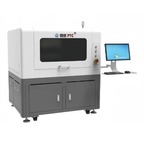
At Suzhou PTC Optical Instrument Co., Ltd., we specialize in providing advanced SAT solutions tailored to meet the demanding needs of the semiconductor industry. Our cutting-edge equipment offers unparalleled defect detection, ensuring that your products meet the highest standards of quality control. Whether you're looking to integrate SAT into your existing production process or need customized solutions for specific testing requirements, we are here to assist you. For more information or to discuss how we can support your testing needs, feel free to reach out to us today. Let us help you enhance your manufacturing processes and ensure the reliability of your products.
SAT is highly effective at detecting internal defects such as voids, cracks, delamination, and material inhomogeneity.
Unlike traditional visual or X-ray methods, SAT provides non-destructive, high-resolution images that offer a more accurate representation of internal structures.
SAT is highly versatile and can be used for various semiconductor materials, including silicon, compound semiconductors, and multi-layered substrates.
By identifying defects early, SAT minimizes waste, rework, and product failures, leading to long-term cost savings in manufacturing processes.


