Please Choose Your Language


Ceramic printed circuit boards operate in highly demanding environments today. Aerospace systems, high-power LEDs, and electric vehicle modules rely on them completely. These sectors demand flawless performance under extreme thermal and mechanical stress. Material costs for these non-organic components are exceptionally high. Scrap rates quickly become a major commercial liability for manufacturers. Standard optical inspection platforms remain ubiquitous in traditional FR4 board manufacturing. However, they struggle immensely when processing highly reflective materials. The unique physical and optical properties of ceramics demand specialized technology. To protect margins and ensure compliance, manufacturing facilities must transition to dedicated systems. Advanced optical platforms can handle highly reflective surfaces accurately. They identify specific defect types unique to these robust yet fragile materials. Manufacturers must adopt targeted inspection technology to navigate the brittle nature of ceramic substrates effectively. We will explore how modern inspection tools secure profitability in zero-defect industries.
Standard AOI systems struggle with the high reflectivity and unique defect profiles of ceramic materials, leading to unacceptable false call rates.
Specialized ceramic substrate AOI equipment uses advanced multi-spectral lighting and AI algorithms to detect micro-cracks, oxidation, and contamination without damaging the substrate.
Evaluating ceramic substrate inspection equipment requires a strict framework balancing optical resolution, handling mechanisms, and integration capabilities.
Deploying single unit AOI equipment provides a scalable, lower-risk entry point for facilities handling variable batch sizes before committing to fully inline automation.
Standard platforms simply cannot read non-organic boards accurately. Alumina (Al2O3) and Aluminum Nitride (AlN) substrates create intense surface glare. This reflection confuses conventional camera sensors entirely. Standard AOI equipment relies on simple white light or basic RGB ring arrays. These conventional setups wash out the image over shiny metalized traces. Critical defects remain hidden beneath the glare. Worse, harmless surface variations trigger false rejects constantly. Standard cameras see substrate grain as contamination. This misinterpretation halts production lines unnecessarily.
The topography of non-organic faults differs vastly from traditional copper-clad FR4 defects. You need to identify microscopic micro-cracks accurately. These tiny fractures compromise the structural integrity of the entire module. Precise laser via alignment is absolutely critical for thermal management. Thick-film printing often suffers from inconsistent edge definitions and screen mesh marks. Standard systems fail to recognize these unique structural anomalies. Traditional template-matching software cannot process the natural variance of fired ceramics.
Inaccuracy destroys profitability in high-reliability manufacturing sectors. Missed defects, known as escapes, cause catastrophic field failures eventually. A single failure in an EV power module damages brand reputation irreparably. Aerospace contracts vanish instantly following a single component failure. Conversely, high false call rates waste expensive raw materials. Engineers lose countless hours manually reviewing rejected boards under microscopes. The financial drain forces factories to seek better solutions immediately. You cannot afford to rely on incompatible inspection technology.
Modern inspection platforms solve reflective challenges through sophisticated optical engineering. Specialized lighting configurations neutralize harsh surface glare completely. Coaxial lighting illuminates deep vias and laser-drilled holes evenly. Low-angle illumination highlights raised surface contamination effectively. Phase-stepping techniques capture three-dimensional topographical data accurately. This multi-angle approach isolates metallization flaws from harmless substrate grain. You gain a perfectly clear image of the true surface structure.
Hairline fractures severely degrade the thermal conductivity of AlN boards. Detecting these microscopic faults requires superior sensor integration. Sub-micron pixel resolution is absolutely essential for this task. Standard cameras simply cannot resolve these minute details. They ensure every conductive path meets stringent automotive standards. High-resolution sensors reveal print bleed and paste smearing instantly. This clarity allows engineers to correct printing parameters before batch failures occur.
Hardware alone cannot solve the persistent false call problem. Algorithmic defect classification provides the critical intelligence layer. Modern ceramic substrate AOI equipment leverages machine learning effectively. Developers train these AI models specifically on vast libraries of non-organic defects. The software learns to differentiate between harmless aesthetic variations and actual structural flaws. Deep learning neural networks adapt to new product runs quickly. This intelligence reduces false rejects drastically while maintaining strict quality control. Operators trust the machine to make accurate pass-or-fail decisions.
Selecting the right platform requires careful analysis of multiple operational variables. Decision-makers must balance optical performance with physical handling capabilities. You must evaluate these machines under strict real-world conditions.
The relationship between defect detection and false call rate (FCR) is critical. You must demand an aggressive FCR trade-off evaluation. A trustworthy system must prove its reliability in your actual production environment. Vendor demonstrations often use perfectly clean, optimized test panels. Real factory conditions introduce dust, vibration, and unpredictable substrate warping. You need equipment that maintains high accuracy during demanding production shifts. A low escape rate means nothing if the machine rejects every good board.
Physical handling mechanisms demand rigorous scrutiny during the evaluation phase. Alumina and Aluminum Nitride boards chip very easily under stress. Rough conveyor belts destroy fragile board edges instantly.
Touchless transport systems protect expensive panels from mechanical stress.
Vacuum-assisted holding platforms prevent micro-abrasions on the bottom surface.
Specialized edge-handling automation remains a non-negotiable requirement.
Soft-stop mechanisms prevent impact damage during station transfers.
Any reliable Ceramic Substrate Surface Inspection Equipment must guarantee zero physical damage during transport.
Factories must balance throughput expectations against resolution requirements carefully. Capturing sub-micron images takes significant computational time. You cannot scan a panel at nano-scale resolution in two seconds. Engineers must calculate realistic inspection cycle times based on production demands.
Throughput vs. Resolution Trade-off Framework
Resolution Range (µm) | Field of View (FOV) | Processing Speed | Ideal Factory Application |
|---|---|---|---|
0.5 - 1.0 | Extremely Narrow | Low (Offline Analysis) | Aerospace, Micro-cracks |
2.0 - 5.0 | Medium | Moderate | High-Power LED, Thick-film |
10.0+ | Wide | High (Inline Production) | Basic Macro-Defect Sorting |
Use this framework to align the camera capture speed with your factory takt time. A mismatch here creates massive bottlenecks on the production floor.
Factories must choose the right physical footprint for their production strategy. High-volume continuous manufacturing requires robust inline integration. These fully automated systems sit directly after the screen printers or firing kilns. They scan every single board without human intervention. Inline machines must comply with strict industry communication protocols. SMEMA and Hermes standard compliance ensures seamless conveyor hand-offs between different vendors. Robotic loading mechanisms feed panels continuously to maximize throughput.
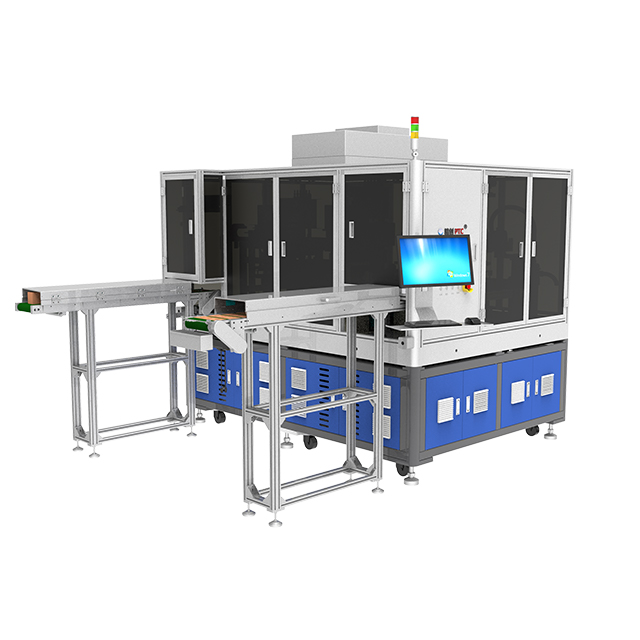
However, many facilities do not run continuous mega-batches. High-mix, low-volume (HMLV) environments face entirely different operational challenges. Here, deploying single AOI equipment is often the most strategic choice. Research and development labs need flexible testing environments daily. Standalone units allow engineers to inspect variable batch sizes easily. They provide a lower-risk entry point to validate return on investment. You can prove the technology works before committing capital to fully inline automation.
Smart factories build a clear scalability path for their inspection capabilities. You can start small and expand as production demands increase.
Deploy a standalone unit for initial process validation and testing.
Train internal engineers on recipe creation and AI model tuning.
Upgrade optical heads when smaller defect resolution becomes necessary.
Unlock network software licenses to link multiple offline systems together.
Transition to full inline automation once production volume justifies the footprint.
This phased approach protects your capital while building internal technical competence.
Buying the machine is only the first step toward zero-defect manufacturing. High-precision optical inspection requires strict environmental controls. Temperature fluctuations warp metal chassis slightly. This throws off micron-level optical calibrations entirely. Micro-vibrations from nearby stamping presses blur high-resolution image captures. Dust particles settling on reflective panels trigger false defect alarms constantly. You must isolate the equipment properly to maintain measurement accuracy. Many factories build dedicated Class 10k cleanroom enclosures for their inspection tools.
Do not underestimate the operator training burden. Standard optical systems often run on simple, template-matching software. Operators learn these basic interfaces in a few hours. Specialized platforms require higher-tier engineering oversight. Technicians must understand phase-stepping illumination and complex thresholding techniques. Creating reliable inspection recipes takes deep material knowledge. Tuning AI algorithms requires patience and consistent data labeling. You must invest in comprehensive metrology training for your quality control team.
Unintegrated inspection data creates dangerous operational blind spots. Data silos prevent root-cause analysis across the production floor. If the machine finds a defect, it must tell the factory why it happened.
Avoid using isolated local hard drives for critical data storage.
Emphasize the need for open APIs in your software evaluation.
Ensure SECS/GEM compatibility for seamless factory-wide communication.
Feed defect coordinate data back to screen printers immediately.
This closed-loop process correction stops defects before they multiply. It transforms the inspection machine from a passive filter into an active quality controller.
Investing in dedicated inspection technology remains a critical risk-mitigation strategy for modern factories. Standard visual systems simply cannot secure contracts in zero-defect industries. Upgrading your optical capabilities protects high-value materials from unnecessary scrap. It ensures compliance with stringent automotive and aerospace manufacturing standards. You eliminate escapes and protect your brand reputation from field failures.
Your strategic action plan should focus on rigorous physical validation. Request a Proof of Concept (PoC) from potential vendors immediately. Do not rely on standard vendor test boards during this evaluation phase. Ship your own most challenging, defective panels to the vendor directly. Evaluate their algorithmic accuracy on your specific material variations. Start with standalone units to validate the workflow before scaling to full inline automation.
A: Standard systems use basic RGB lighting and simple template matching designed for dull FR4 surfaces. Ceramic systems focus on advanced lighting architecture like coaxial and phase-stepping arrays. These neutralize harsh surface glare. They integrate micron resolution sensors. They also rely on AI algorithms specifically trained for non-organic, highly reflective substrates.
A: Yes, but the method varies by machine design. Basic standalone units require operators to flip the panels manually for the second pass. Advanced offline machines feature automated dual-camera setups. These capture both the top and bottom surfaces simultaneously. This greatly increases throughput without risking manual handling damage.
A: High-temperature firing often causes substrate camber or warping. Specialized inspection systems use 3D optical profiling to map the surface topology before scanning. They employ dynamic Z-axis autofocus mechanisms to adjust the camera lens in real-time. This compensates for height variations perfectly. It keeps microscopic defects in sharp focus.