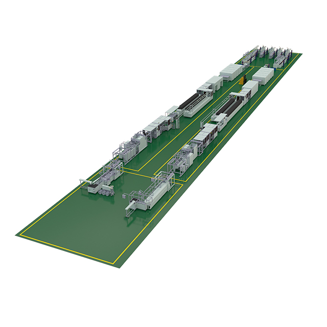
In sensor manufacturing, a small soldering defect or coating flaw can lead to unstable performance, poor appearance, or later quality complaints. For temperature sensor chips, manual checking is often too slow and inconsistent, especially after soldering and coating. This is why Sensor Integrated Line Fully Automated Equipment should be understood as anAutomatic Surface Defect Inspection Solution designed to connect with a customer’s existing production flow. It focuses on visual inspection, defect recognition, dimensional checking, data traceability, and inspection-result feedback. It is not positioned as an equipment package for building or assembling the customer’s product.
For PTC applications, the key value of this equipment is its ability to support automatic AOI inspection for temperature-sensing chip components. After soldering, the system can inspect cosmetic defects such as short circuit, open circuit, chip misalignment, insufficient solder, oxidation, cracked components, missing components, and bulging. After coating, it can inspect coating surface defects and key dimensions such as coated length and outer diameter. This makes the system especially useful for manufacturers that need stable, repeatable, in-line surface inspection before products move to the next process.
What the Equipment Means for Sensor Chip Inspection
The name may sound broad, but the practical function is clear: the equipment provides automated surface inspection and inspection-related handling for temperature sensor chip components. It can be docked with the customer’s production line so that inspected products move through the checking station with less manual intervention. In this role, the equipment acts as a quality gate. It checks whether soldering and coating results meet the defined inspection standards before the components continue to the next operation.
Compared with a standalone manual inspection table, a connected AOI system brings three clear advantages. First, it improves consistency because the same inspection logic is applied to every part. Second, it supports faster inspection for high-volume production. Third, it creates digital records that can support yield analysis, batch tracking, and process improvement. The official sensor chip surface inspection equipment page describes AOI functions for chip soldering defects, continuous soldering cosmetic defects, coating surface defects, and coating dimension inspection.
Why Temperature Sensor Chip Surface Inspection Matters
Temperature sensor components are often small, precise, and sensitive to process variation. A solder bridge may create an electrical problem. Insufficient solder may reduce connection reliability. Chip rotation or misalignment may affect later assembly accuracy. Coating bubbles, dirt, pinholes, scratches, deformation, or abnormal coating thickness can also create risk in appearance, protection, or downstream fitting. These problems may not be easy to judge by eye when production speed increases.
Automatic visual inspection helps manufacturers find these issues earlier. Instead of relying only on final checks, the inspection station can evaluate the part soon after soldering and coating. This allows the production team to separate NG products, review defect trends, and adjust the upstream process in time. In other words, the equipment is not only a checker. It also becomes a source of process feedback.
Main Inspection Items After Chip Soldering
Soldering inspection is one of the most important parts of sensor chip quality control. After the chip is soldered, the AOI system captures high-resolution images of the soldering area and compares real product features with preset inspection rules. If a defect is found, the software marks the defect position and records the result.
For temperature sensor chip soldering, common inspection items may include short circuit, open circuit, insufficient solder, cracked component, oxidation, missing component, external and internal misalignment, and bulging. For continuous soldering areas, inspection can also include insufficient clearance, cold solder joint with exposed lead, excessive solder on the lead, lifted lead, solder bump, and component body length measurement. These checks are important because soldering defects are often connected with both appearance quality and product reliability.
How AOI Identifies Soldering Defects
AOI inspection begins with stable part positioning. Once the component reaches the inspection area, the imaging system captures the solder joint, chip body, and surrounding area under controlled lighting. Then the software analyzes shape, edge, brightness, size, and position information. When the result is outside the preset tolerance, the system can mark the suspected defect for review. In AI-supported applications, model training can also help filter false defects and improve the useful defect-recognition rate over time.
Coating Surface Defect and Dimension Inspection
After coating, inspection needs to cover both surface defect and size. Coating surface problems may include bubbles, dirt, deformation, pinholes, and surface scratches. Dimension inspection may include overall coated length, coating outer diameter at the joint section, and coating outer diameter around the chip mounting area. These inspection points are highly relevant to temperature sensor chip applications because coating quality affects the part’s protection, appearance, and later compatibility with the customer’s process.
The equipment can support automatic checking of these coating-related items without turning the article into a discussion about coating production itself. The focus remains on inspection. The customer may already have soldering, coating, curing, and transfer processes in place. PTC’s role is to provide the appearance inspection equipment that can be connected to that process and help confirm whether the finished soldering or coating result is acceptable.
How the Inspection Equipment Connects to Customer Lines
In real factory use, inspection equipment rarely works as an isolated island. It needs to receive products from the previous process and send checked products to the next process. This is why line docking is important. The equipment can be configured to work with customer-side material handling, loading and unloading methods, and information systems. The goal is to create a smooth inspection station inside the customer’s own manufacturing flow.
For this reason, the correct wording is important. PTC provides surface defect detection equipment for line integration, not a general product-building system. The equipment may include inspection-related motion, transfer, positioning, and data communication functions, but its main business value is AOI appearance inspection. Manufacturers can explore the wider intelligent inspection equipment category when they need to compare different inspection and automated detection applications.
Software, Data, and MES Connection
Modern AOI equipment should do more than capture images. It should also help the production team understand results. The software layer can display the real-time inspection process and final inspection results. It can save production data, batch information, and yield statistics. It can also support query and export functions, including export to Excel for later review.
MES integration is another practical feature for factories that need traceability. When inspection results are connected with manufacturing data, quality teams can review which batch, model, or process condition created a defect trend. This supports faster root-cause analysis and makes quality management easier to scale across high-volume production.
AI-Assisted Defect Marking and Model Training
Some defects are clear and easy to define, while others are more difficult. For example, dirt, small scratches, slight deformation, or borderline soldering features may look different from part to part. AI-assisted software can help by marking defects, supporting model training, and filtering false defects. This does not replace process knowledge. Instead, it helps engineers improve recognition rules as more inspection data is collected.
This is especially useful when customers run different product models. If the equipment supports template creation and parameter configuration, engineers can set suitable inspection standards for different products. This improves flexibility while keeping inspection logic controlled and repeatable.
Key Specifications to Review Before Selection
Before selecting AOI equipment for temperature sensor chip inspection, manufacturers should review whether the inspection items match their real process. A good selection process should begin with actual defect samples, coating surface inspection requirements, soldering quality rules, and expected line speed. The inspection system should be evaluated not only by camera resolution or software functions, but also by whether it can reliably detect the defects that matter most in the customer’s process.
Selection Point
What to Confirm
Why It Matters
Inspection items
Soldering cosmetic defects, coating cosmetic defects, and coating dimensions
Ensures the equipment matches temperature sensor chip quality requirements
Product compatibility
Template creation and parameter setup for different models
Supports product changeover and model variation
Data management
Result display, query, export, and batch/yield statistics
Improves traceability and quality analysis
Line docking
Loading/unloading method and connection with customer-side handling
Helps the inspection station fit the existing production flow
False-defect control
AI marking, model training, and overkill control
Reduces unnecessary rejection and improves practical inspection value
Recommended Product Reference
For this application, the most relevant product reference is PTC’s AOI equipment for Soldering and Coating Defect Inspection. This product page lists inspection items for chip soldering cosmetic defects, continuous soldering cosmetic defects, coating cosmetic defects, and coating dimension inspection. It also describes software functions such as real-time result display, production data statistics, data saving, data query, and Excel export.
For customers working with temperature sensor components attached with paper tape or similar component forms, the Matsuba component AOI inspection application may also be useful as a related reference. It highlights soldering cosmetic inspection, dimension inspection, coating cosmetic inspection, data query, export, analysis, MES integration, and AI-supported defect marking. These functions are closely connected with the same inspection logic used in sensor component appearance quality control.
What Information Customers Should Prepare
To build a reliable inspection plan, customers should prepare several types of information before technical discussion. These include product drawings, soldering area images, coating area images, defect samples, OK/NG judgment standards, required inspection speed, loading and unloading conditions, and data connection needs. If MES connection is required, the communication format and data fields should also be clarified early.
Clear input information helps engineers design better inspection logic. For example, if the main concern is insufficient solder, the imaging and rule settings should focus on solder volume, edge shape, and exposed conductor features. If coating dimension is the main concern, the system should focus on stable measurement, repeatability, and tolerance control. This makes the inspection station more useful from the first production trial.
Benefits for Quality Control
When used correctly, sensor chip surface inspection equipment can help manufacturers improve quality control in several practical ways. It reduces dependence on manual visual judgment, supports full-process inspection records, and helps detect process drift earlier. It can also help engineering teams compare defect types by batch, shift, model, or process condition.
The result is not only better inspection speed. More importantly, manufacturers gain a clearer view of what is happening after soldering and after coating. Defects become measurable, searchable, and easier to analyze. This is why automatic surface defect inspection is becoming a key part of stable sensor component manufacturing.
Conclusion
Sensor Integrated Line Fully Automated Equipment is best understood as an automated AOI Surface Defect inspection solution for temperature sensor chip applications. It is used to connect with the customer’s existing production flow and check critical visual and dimensional quality points after soldering and coating. It does not mean that PTC provides a complete product-assembly system.
For manufacturers of temperature sensor chips and related sensor components, the system can support soldering defect inspection, coating appearance inspection, coating dimension inspection, AI-assisted defect marking, data export, and MES-ready quality management. With the right defect samples and process requirements, it can become a reliable inspection station that improves consistency, traceability, and production confidence. To discuss a specific application, customers can share sensor chip inspection requirements with PTC for further technical evaluation.
FAQ
Q1: Is Sensor Integrated Line Fully Automated Equipment used for product assembly?
No. In this application, it should be understood as surface defect inspection equipment that can be docked with the customer’s existing production line. The focus is automatic AOI inspection for temperature sensor chip soldering and coating quality.
Q2: What defects can it inspect after temperature sensor chip soldering?
It can inspect soldering-related cosmetic defects such as short circuit, open circuit, misalignment, insufficient solder, oxidation, cracked component, missing component, bulging, solder bump, lifted lead, and other visible soldering issues defined by the customer’s quality standard.
Q3: Can it inspect coating defects?
Yes. The equipment can support coating cosmetic inspection for defects such as bubbles, dirt, deformation, pinholes, and surface scratches. It can also support coating dimension checks, including coated length and outer diameter measurements.
Q4: How does the equipment connect with a customer production line?
It can be configured as an inspection station that receives products from the previous process and sends checked products to the next process. Docking details depend on the customer’s loading, unloading, material handling, and data communication requirements.
Q5: Does the system support data export?
Yes. The software can support inspection result display, production data statistics, batch information, yield statistics, data saving, query, and export functions. This helps quality teams review results and trace batch performance.
Q6: What should customers provide before selecting an AOI solution?
Customers should provide product samples (OK and NG samples), defect definitions, coating size requirements, required inspection speed, line docking conditions, and data connection needs. These details help create a more accurate inspection plan.
 English
 العربية
 Français
 Русский
 Español
 Português
 Deutsch
 italiano
 日本語
日本語 한국어
한국어 Nederlands
 Tiếng Việt
 ไทย
ไทย Polski
 Türkçe
 Bahasa Melayu
 தமிழ்
தமிழ் Filipino
 Bahasa Indonesia
 magyar
 Română
 Čeština
 Српски
 हिन्दी
 فارسی
فارسی Slovenčina
 Slovenščina
 українська
 Suomi
Suomi Հայերեն
 עברית
עברית Latine
 Shqip
Shqip বাংলা
বাংলা Eesti keel
 Oʻzbekcha
 latviešu
 Беларуская мова
 Esperanto