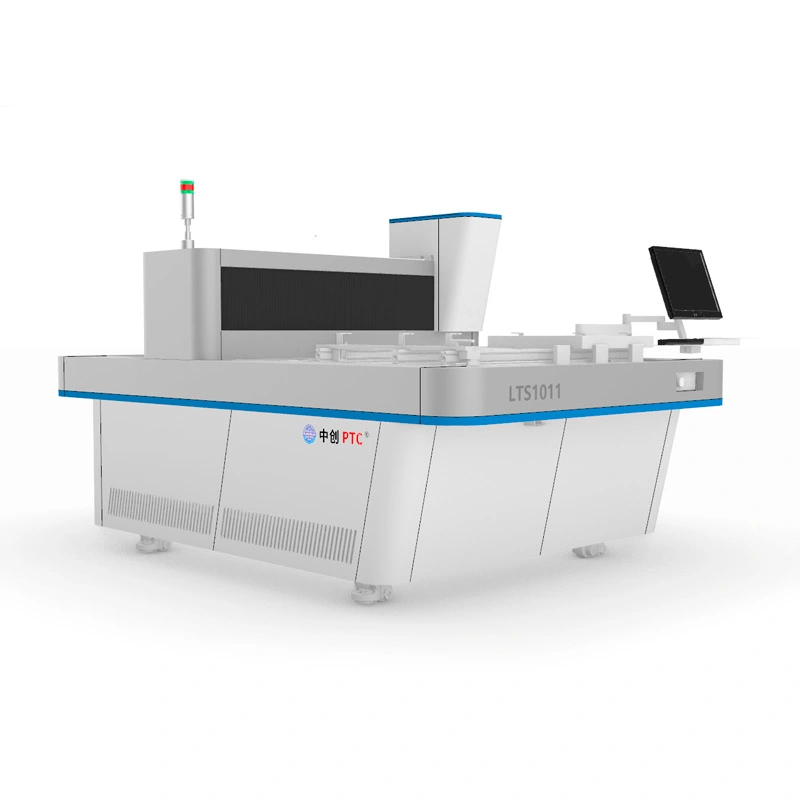
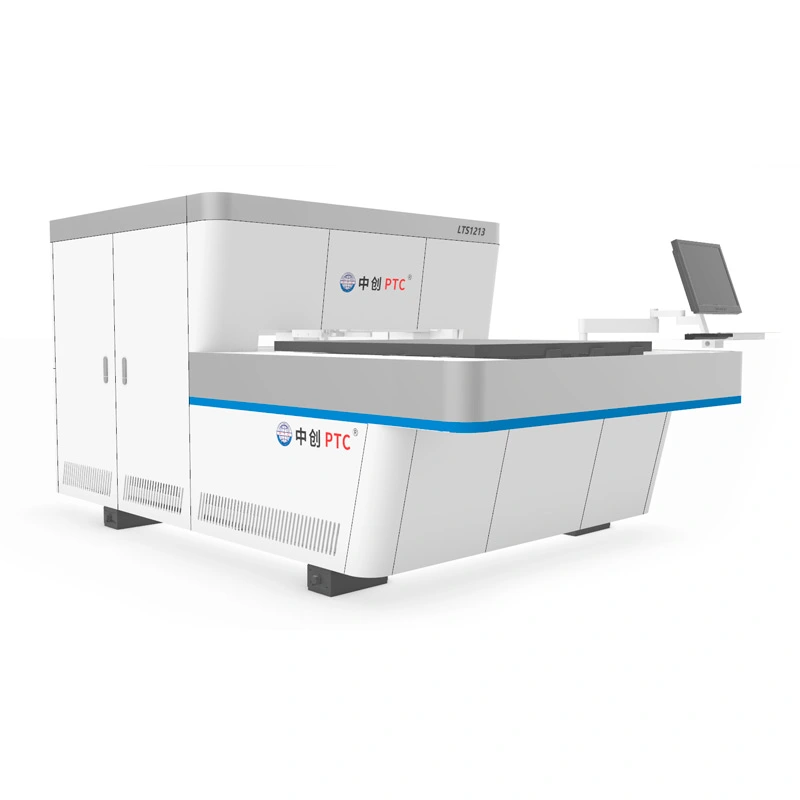
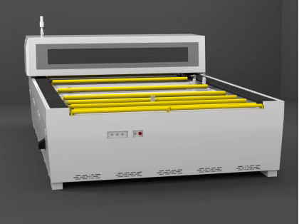
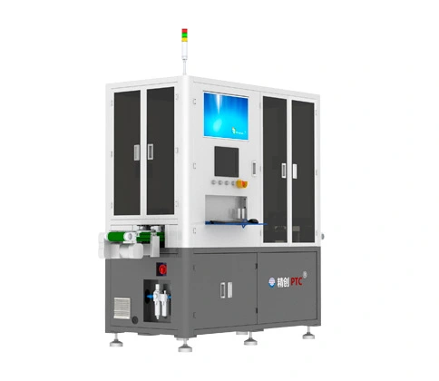
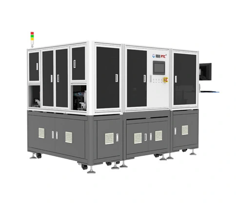
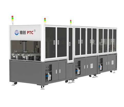
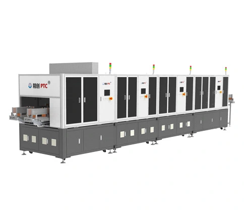
Features of Laser Direct Imaging Equipment
High accuracy: Resolution 1270dpi /2540dpi, 133 LPI.
High efficiency: 3 minutes to expose a 1000mm*1000mm screen; Precise exposure alignment to greatly saves preparation time, reduces labor and saves time.
Low cost: Adopting DMD direct imaging technology, there is no need for film. There are no quality problems caused by film wear and unstable expansion and contraction, while the cost is reduced. The three steps of traditional film exposure are shortened into one step of LTS laser direct plate making, achieving the purpose of fast, accurate and low-cost plate making.
Specifications
LTS1011 Direct Imaging Equipment Technical Parameter |
Max frame dimension | 1100 mm*1100 mm |
Min frame dimension | 400mm*400mm |
Max exposure area | 1000mm*1000mm |
Frame thickness (can be customized) | 25-45mm |
Imaging System Technology | DMD DLP Technology |
Emulsion thickness (EOM) | solvent type sensitive emulsion: 3μm-160μm, water type sensitive emulsion: 3μm-240μm |
Exposure time | 160-200S/m²( film thickness12-15um ) 200-240S/m² (film thickness 20-25um) SBQ type photosensitive emulsion |
Resolution | 1270dpi / 2540dpi (optional), 12700dpi (for PCB) |
Line number per inch | 133LPI |
Focusing method | dynamic real-time focusing |
File format | Gerber274x, 1-Bit-Tiff |
Laser type | UV laser, wavelength 405±5nm |
Laser power | 20W/25W/30W(optional) |
Dimension | 2680 mm*1580 mm*1500 mm |
Net weight | 2200KG |
Working environment | yellow light room; clean-room level: 10000; temperature 22±2°C, 60-70% relative humidity (no condensation) |
Power electricity, air pressure | single-phase 220V, 50/60HZ, 4KW, air 1L/min |
Applications of Laser Direct Imaging Equipment
1. Printing-related Field: This includes textiles, printing, packaging, and label making. It can create high-precision patterns, meet different printing requirements, and enhance printing quality and visual effects.
2. Manufacturing Industry: In automotive glass manufacturing, it accurately prints patterns and logos. In decorative panel processing, it creates patterns to increase product added value.
3. Electronics Field: For circuit board production, it realizes the exposure and imaging of fine circuits. In the production of ceramic substrates and thick film circuits, it meets high-precision manufacturing requirements and improves circuit performance.

 EN
EN
 ko
ko  fr
fr  de
de  es
es  it
it  ru
ru  pt
pt  ar
ar  hi
hi  jw
jw  zh-CN
zh-CN
