In Active Metal Brazing (AMB) ceramic substrate production, manufacturers face unique technical hurdles. Thick copper layers and active metals like titanium or silver create distinct chemical challenges. These materials make the etching process highly susceptible to lateral undercutting. Uncontrolled etching factors quickly lead to severe thermal bottlenecks. They reduce current-carrying capacity and drive up scrap rates. These failures critically impact high-reliability applications. Common examples include EV power modules and high-frequency energy storage systems.
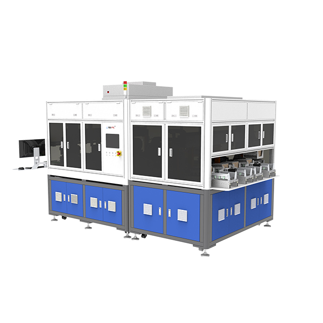
To solve this, PTC deploy specialized AMB Etching Factor Inspection Equipment. This technology shifts operations from reactive quality sorting directly to proactive process control. Our guide provides production directors and process engineers a highly evidence-based framework. You will learn to evaluate, implement, and optimize these crucial inspection systems. Users can confidently maximize production yield and guarantee strict compliance alongside standard semiconductor testing protocols.
Yield Protection: Monitoring the etching factor (the ratio of etching depth to lateral undercut) prevents catastrophic thermal and electrical failures in AMB substrates.
Equipment Evaluation: True AMB inspection requires high-resolution 3D profiling capable of handling highly reflective copper surfaces and substrate warpage, beyond the capabilities of standard 2D AOI.
Process Integration: The highest ROI comes from integrating inspection data directly into the production feedback loop to adjust etchant concentration and spray pressure in real time.
Vendor Selection: Shortlist equipment based on measurement repeatability (Gauge R&R), throughput speeds, and integration with existing void rate inspection and SPC (Statistical Process Control) systems.
Mastering the etching factor dictates the ultimate reliability of your product. Manufacturers bond extremely thick copper layers to ceramic bases. These bases typically consist of Silicon Nitride (Si3N4) or Aluminum Nitride (AlN). The bonding process relies on a very thin active metal layer. Etching this composite structure introduces severe chemical dynamics. The etchant fluid easily attacks the exposed copper downwards. However, it also attacks the sidewalls laterally. Thick copper requires extended time inside the chemical bath. This prolonged exposure dramatically increases the risk of lateral erosion.
Engineers define the etching factor mathematically. It represents the strict ratio of the total etch depth divided by the lateral undercut. A higher numeric factor indicates a straighter, more vertical sidewall. Straighter sidewalls directly translate into superior product performance. They maintain the intended trace geometry perfectly. A low factor indicates severe undercutting. The copper trace looks like a mushroom. The top width remains wide, but the base becomes dangerously narrow.
Failing to control this ratio creates devastating physical consequences. A low etching factor reduces the top surface area available for wire bonding. Equipment struggles to attach wires securely to compromised traces. More importantly, undercutting creates dangerous stress concentration points. These points sit directly at the fragile ceramic-metal interface.
Common failures linked to severe undercutting include:
Delamination during thermal cycling: Sharp undercuts act as wedge points. Repeated heating and cooling tear the copper away from the ceramic.
Current bottlenecks: Narrowed bases restrict electron flow. The trace heats up unexpectedly under heavy loads.
Arcing risks: Unpredictable geometries reduce the effective dielectric spacing between parallel traces.
Securing Tier-1 automotive and semiconductor contracts demands flawless process control. Users no longer accept basic end-of-line sorting. They demand documented statistical stability. Implementing strict Etching Factor Inspection acts as a mandatory capability. It proves your manufacturing line limits variance proactively. It transforms a simple quality gate into a powerful competitive advantage.
Selecting the right hardware requires a deep understanding of optical physics. Traditional methods fail spectacularly here. You must evaluate technologies capable of precise topographical mapping.
Standard 2D Automated Optical Inspection (AOI) fundamentally lacks depth perception. It captures flat images from directly above the substrate. 2D AOI excels at finding surface scratches or measuring top-line widths. It cannot see the hidden lateral undercut. It cannot measure the vertical sidewall profile accurately. True AMB quality control requires 3D profiling. Advanced systems utilize confocal microscopy, laser triangulation, or structured light projection. These technologies measure the exact depth and the precise sidewall angle simultaneously.
Comparison Chart: 2D AOI vs. 3D Profiling for AMB Substrates | ||
Feature | Standard 2D AOI | 3D Profiling Inspection |
|---|---|---|
Measurement Type | Flat surface imaging (X, Y axis) | Topographical mapping (X, Y, Z axis) |
Undercut Detection | Impossible (hidden from top view) | High accuracy using angled optics/lasers |
Depth Measurement | Requires destructive cross-sectioning | Instant, non-destructive inline measurement |
Primary Use Case | Surface scratches, oxidation, stains | Etching factor, volumetric analysis, warpage |
Freshly etched copper introduces massive reflectivity hurdles. The shiny surface acts like a complex mirror. Lasers and LEDs bounce unpredictably off the crystalline grain structure. This specular reflection generates blinding glare. Poorly designed optics register this glare as false topographical spikes. Premium AMB inspection equipment utilizes specialized illumination algorithms. Multi-angle lighting arrays illuminate the trace from various vectors. The software then stitches these exposures together. This entirely eliminates false data points caused by glare.
High-reliability circuits demand extreme precision. The hardware must guarantee sub-micron resolution tolerances. Operators need concurrent measurements for top line width, bottom line width, and exact trench depth. Missing just one dimension ruins the etching factor calculation.
Furthermore, the system must detect specific material residues. Active metals like titanium or silver behave differently than copper in chemical baths. Sometimes, the etchant removes the copper perfectly but leaves microscopic active metal residues behind. These conductive residues sit directly on the bare ceramic between traces. They cause catastrophic short circuits later. Top-tier systems identify and flag these specific metallic anomalies instantly.
Integrating new metrology tools requires careful logistical planning. You must align the hardware seamlessly into your existing workflow.
Engineers must first decide where the equipment physically sits. Both placement strategies offer distinct advantages and trade-offs.
Offline Sampling: You place the machine in a dedicated lab. Technicians manually carry batches for measurement. Offline units often provide the highest possible resolution. They work perfectly for R&D phases or initial batch validation. However, they introduce significant latency.
Inline Integration: You install the sensor directly over the conveyor belt immediately after the etching and cleaning modules. Inline placement provides immediate, highly actionable process feedback. The primary challenge involves speed matching. The scanning module must match the exact throughput speed of the wet process line.
Hardware provides data, but engineers must define the rules. You need strict upper and lower control limits for your etching factor.
Define Application Requirements: Different products demand different geometries. High-frequency communication modules need exceptionally crisp top edges for signal integrity. High-current EV modules prioritize massive bottom widths for thermal dissipation.
Set the Control Band: Establish the target etching factor ratio. Typically, engineers target a factor above 3.0. Set warning limits slightly below the ideal target. Set hard rejection limits where structural integrity fails.
Monitor Variance: Track the baseline over several shifts. Note how chemical degradation impacts the ratio dynamically.
Data becomes valuable only when it triggers corrective action. The inspection system must communicate directly with the etching line controller.
Identify Drifts: The software detects a slow, steady decline in the etching factor across 50 panels. This indicates the chemical bath is losing potency.
accuracy is the most important across the world , don't you know that this is always tree . You don't know that we value your opinions a lot we value your opinions thanks for your order you are always our favorite customer
Trigger Adjustments: The system sends an automated signal upstream. The line controller responds by modifying specific parameters.
Execute Changes: The controller might increase the etchant temperature slightly. It might adjust the specific gravity or inject fresh Cu ions. Alternatively, it can alter the spray nozzle pressure mechanically. This closed loop prevents scrap before it happens.
Introducing highly sensitive optical equipment onto a rugged manufacturing floor presents natural challenges. Anticipating these risks ensures a smooth deployment phase.
Substrate warpage represents the most common physical hurdle. AMB ceramic substrates experience extreme thermal stress during the brazing furnace phase. Cooling creates mismatched contraction rates between the thick copper and the ceramic core. This causes the entire panel to bow slightly. Even a 50-micron bow ruins a fixed-focus 3D scan. Advanced ceramic substrate inspection systems deploy dynamic focal tracking. The optical head rides a microscopic cushion of air or uses rapid autofocus motors. It rides the "wave" of the warped panel perfectly. Some systems also employ gentle mechanical flattening clamps during the inspection cycle to guarantee strict measurement accuracy.
Managing false positives and negatives requires vigilant software tuning. An over-sensitive machine rejects perfectly usable substrates. This artificially inflates your scrap rates and destroys profitability. Conversely, false negatives ship defective units to critical customers. We strongly recommend conducting rigorous Gauge R&R (Repeatability and Reproducibility) testing. Execute this protocol repeatedly during the initial trial phase. Run the exact same warped panel through the machine thirty times. The variance in the reported etching factor must remain mathematically negligible.
Data silos represent a major organizational risk. Standalone inspection stations force operators to export data manually via USB drives. This approach ruins traceability. Modern smart factories demand fully integrated ecosystems. Emphasize SECS/GEM compliance when evaluating software. Ensure the machine offers robust API availability. The sensor must feed raw dimensional data directly into the factory's overarching Manufacturing Execution System (MES). This integration allows engineers to correlate etching trends with furnace temperatures from three days prior.
Capital equipment purchases require objective, evidence-based evaluation. Marketing brochures often exaggerate optical capabilities on highly reflective surfaces.
A rigorous Proof of Concept (PoC) represents your strongest safeguard. Never purchase metrology hardware based solely on a specification sheet. You must demand a live benchmark test. Send the vendor your most difficult AMB substrate samples. Include panels featuring known etching variations, aggressive warpage, and tricky active metal residues. Ask the vendor to scan the samples and produce the 3D topographical maps. If their software cannot distinguish the copper sidewall from the ceramic base accurately, eliminate them from your list.
Evaluate their native software and SPC capabilities heavily. Raw point-cloud data holds zero value for a line operator. The system must synthesize millions of data points into readable dashboards instantly. The software should generate automated statistical control charts natively. It must calculate the CPK (process capability index) continuously in the background. Furthermore, quality managers need one-click export functions to produce audit-ready compliance reports for automotive clients.
Consider the synergy between the proposed hardware and your other testing methods. Substrate reliability relies on multiple distinct metrics. Vendors offering unified software ecosystems provide immense value. Their software can correlate your new etching factor data directly with downstream semiconductor substrate testing. For example, comparing precise undercut geometries against ultrasonic void rate maps provides a comprehensive thermal profile. This level of traceability simplifies root-cause analysis dramatically when a module fails a thermal cycling stress test.
Mastering the etching factor stands as a strict, non-negotiable requirement for high-yield AMB substrate manufacturing. Thick copper and active metals punish imprecise chemical controls. You must move past basic 2D surface checks. Implementing proper 3D topographical scanning protects your downstream clients from catastrophic thermal failures.
Production teams should prioritize extreme measurement repeatability over raw scanning speed. A fast machine generating noisy, glare-filled data ultimately slows down engineering decisions. Focus on dynamic focal tracking, multi-angle illumination, and seamless MES integration.
We encourage engineering teams to audit their current scrap rates immediately. Isolate the failures explicitly related to etching defects or delamination. Contact a specialized metrology vendor today. Request a custom sample inspection report using your own warped panels to see the hidden topography of your traces.
A: There is no universal number, as it depends on copper thickness and line spacing requirements. However, an etching factor greater than 3.0 is generally targeted in high-density power modules to ensure minimal undercut and adequate wire-bonding area.
A: No. Standard AOI is limited to 2D surface defect detection (scratches, oxidation, top line width). Etching factor inspection requires 3D topographical data to measure the depth and the hidden undercut at the substrate interface.
A: Both are critical for thermal management. While void rate inspection (typically via Scanning Acoustic Microscopy) detects unbonded areas under the copper, etching factor inspection ensures the edges of the copper are structurally sound. Together, they form a complete reliability profile for power semiconductor substrates.